RC13. Building an Adder, Part 3
Daily dispatches from my 12 weeks at the Recurse Center in Summer 2023
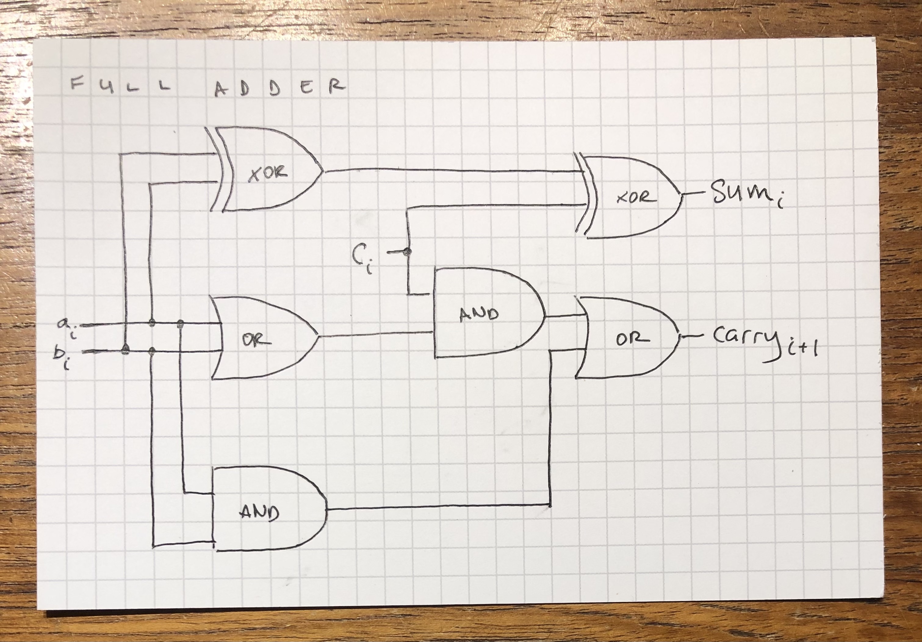
A few days ago I posted the following schematic for a full adder, which I derived algebraically with a fellow recurser:

The HDL for that looks like this:
CHIP FullAdder {
    IN a, b, c;  // 1-bit inputs
    OUT sum,     // Right bit of a + b + c
        carry;   // Left bit of a + b + c

    PARTS:A
    // Sum bit logic
    Xor(a=a, b=b, out=aXorb);
    Xor(a=aXorb, b=c, out=sum);

    // Carry bit logic
    Or(a=a, b=b, out=aOrb);
    And(a=c, b=aOrb, out=cAndaOrb);
    And(a=a, b=b, out=aAndb);
    Or(a=cAndaOrb, b=aAndb, out=carry);
}
But when my friend posted his HDL solution, it looked slightly different.
CHIP FullAdder {
    IN a, b, c;  // 1-bit inputs
    OUT sum,     // Right bit of a + b + c
        carry;   // Left bit of a + b + c

    PARTS:A
    Xor(a=a, b=b, out=aXorb);
    Xor(a=aXorb, b=c, out=sum);
    And(a=c, b=aXorb, out=cAndaXorb);
    And(a=a, b=b, out=aAndb);
    Or(a=cAndaXorb, b=aAndb, out=carry);
}
That’s one fewer gate! Given that an OR gate consists of three NAND gates, in theory this solution is less expensive by three NAND gates, which, for a 16-bit adder, would amount to a savings of 48 NAND gates. Not too shabby.
Drawn out as a schematic, it looks like this:

So what’s going on here? Where did that savings come from?
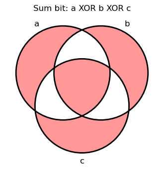
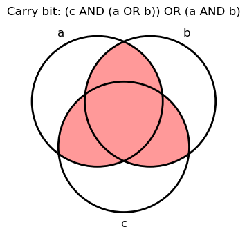
If we look again at the truth tables for the sum and carry bits, we’ll notice that they have something in common, namely \(a \land b \land c\). This is easiest to see with venn diagrams:
| Sum bit | Carry bit |
|---|---|
 |
 |
Let’s revisit this logic.
Notice that the first selection I make for the carry bit at the bottom left is \(a \land b\).

That means all I’m missing are these two yellow areas to get the full logic I need:

To account for the above yellow areas, I ORed the first selection (\(a \land b\)) with \((a \lor b) \land c\).

What you’ll notice now is that I’m essentially double-dipping on the middle section, \(a \land b \land c\), since I’ve selected it twice. I’m not sure that this is a problem in and of itself, however it turns out that elsewhere in the circuit we are actually already creating the missing pieces.
Here’s why. When we’re dealing with the logic for the sum bit, we end up with the following after \(a \oplus b\):

And if we AND the above with c, we end up with the little slices that we need:

Just to be precise, I’ve labeled the above as \((a \oplus b) \lor c\), however the green areas are \((a \oplus b) \land c\).
In any case, now that we have these green intersections, we can add them to the the red intersection with which we began to complete the carry bit logic like so:

That’s how my friend’s revised solution resolves a redundancy in my 6-gate circuit and does the same with 5 gates.
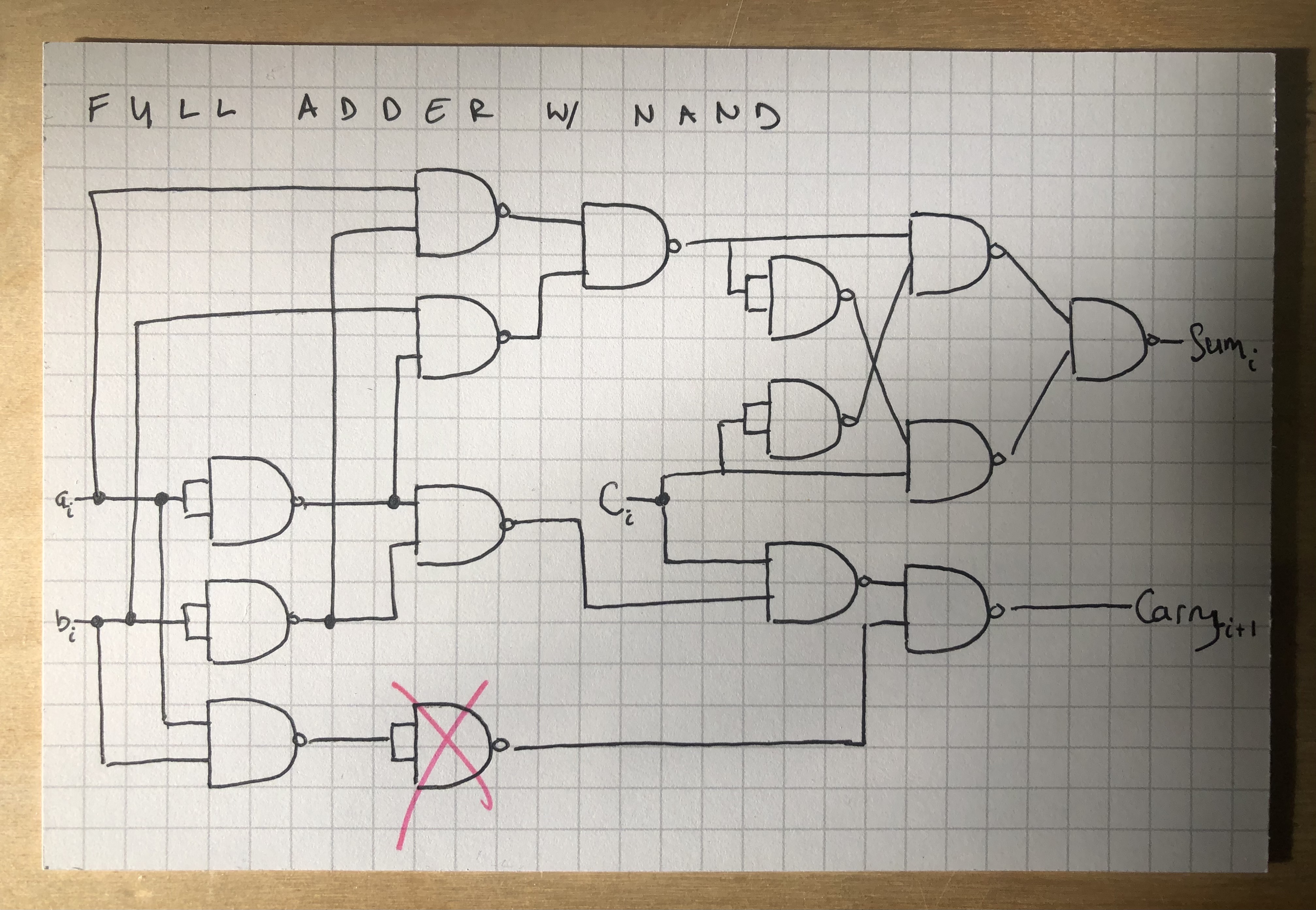
To my credit, when I drew out the 6-gate solution with NANDs, it initially required 20 gates, which I reduced to 14 just from looking for redundacies (things like negated negations, etc.). Here’s my 14-gate NAND adder logic:

As far as I can tell, my friend’s 5-gate solution only requires one fewer NAND gate:

But an improvement is an improvement, so I’ll take it!
What else?
Today was impossible stuff day, but unfortunately I didn’t really get to the impossible stuff I had planned. Won’t make that same mistake next time though.
- made it to checkins
- did a mock technical interview which turned out to go well in spite of feeling like my brain was freezing up at the beginning. It’s definitely hard to think and problem-solve out loud and under the spotlight, but that’s the nature of the beast, I suppose. Anyway, to the extent that technical interviews seemed impossible to me, seems like perhaps I made some progress on an impossible thing after all.
- made some progress on SICP
- finished ALU simulator featured in yesterday’s blog, which I didn’t finish and post until today (time warp)
